| THE HEX SERIES |
Patterned thin films on surfaces
In the production of micro- and nano-fabricated devices, thin films must be deposited in a specific repeating pattern. If this pattern is millimetre-sized or larger, a physical mask, typically fabricated from steel or another inexpensive and easily machined metal, can be placed over the sample to provide shadowing of the substrate, through which the thin film can be deposited in the pattern of the holes in the mask. However, if the required pattern is intricate and requires finer tolerances and features, then a physical mask cannot adequately shadow the deposition flux to produce sharp features on the sample is unsuitable. In these cases, an alternative option known as a lift-off process can be utilised.
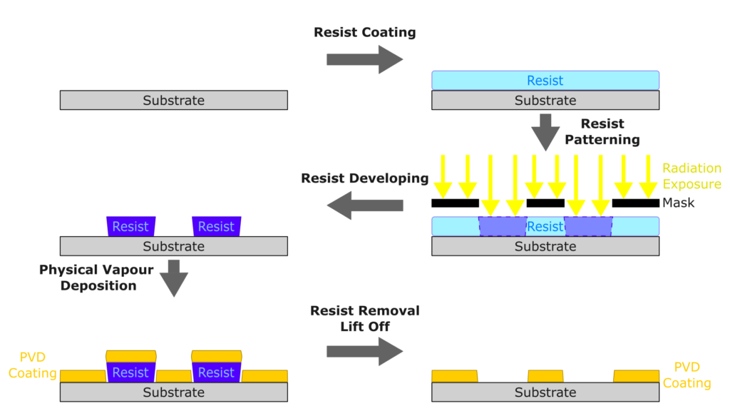
For lift-off, a pattern is developed on the sample substrate commonly by depositing a sacrificial layer of photoresist and exposing this layer to light through a photomask, before etching away the developed resist to reveal the pattern. A PVD coating can then be deposited across the entire sample, onto the substrate where the photoresist has been removed and onto the remaining photoresist. The photoresist is subsequently washed away, revealing the patterned deposition coated directly onto the substrate beneath.
In order to successfully pattern using the lift-off process, several features are required of the PVD system as a whole. The deposition must ideally be done from a point source, perpendicular to the sample (or as close to it as possible), so an extended throw-distance is essential. This configuration minimises the deposition flux incident on the sidewalls of the photoresist and maintains the sharp edge of the mask as much as possible.
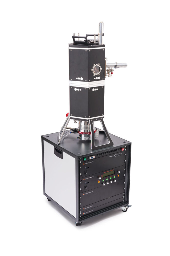
At Korvus Technology, we have developed a unique way to facilitate lift-off applications through the development of our stacked range of modular PVD systems. All the HEX series of PVD chambers can be stacked at any point in their lifetime to increase the distance between the deposition source and sample table. This feature, tied in with our unique TAU mini-electron beam source and range of active and passive-cooled stages, provides the perfect platform for high-quality and simple lift-off deposition runs. We also provide an alternative soft sputtering option that can be used with photoresists. Use the HEX configurator to configure your own deposition chamber and explore your options.
Frequently Asked Questions
What is lift-off in PVD?
Lift-off in PVD (Physical Vapour Deposition) is a patterning technique used to create precisely defined thin-film structures on a substrate. Instead of etching away unwanted material after deposition, lift-off works by depositing material across the wafer and then removing the underlying resist to “lift off” removing the unwanted parts and leaving behind the coated material in the desired pattern.
It is especially useful for fine features, delicate substrates, and materials that are hard to etch, like gold or some oxides.
What are the stages of Lift-off process?
- Resist Coating
A resist layer (usually photoresist or e-beam resist) is spin-coated onto the substrate.
- Patterning
The resist is patterned using photolithography or electron beam lithography (EBL).
In lift-off, it is common to use negative-tone resist or bi-layer resist to create undercut profiles, which help with clean lift-off.
- PVD Deposition
The material (metal, oxide, etc.) is deposited using a PVD technique like:
Thermal evaporation, Electron beam evaporation, or Sputtering (sputtering can be trickier for lift-off due to directional scattering at the intrinsically higher processing pressures).
- Lift-Off (Resist Removal)
The sample is soaked in a solvent (e.g., acetone or PGMEA (propylene glycol methyl ether acetate)) that dissolves the resist.
The material on top of the resist lifts off, leaving behind only the material that was deposited directly onto the substrate.
What Are The Main applications of Lift-off?
Microelectronics: Creating electrical contacts on surfaces and integrated circuits on silicon.
Microelectromechanical systems (MEMS) and microoptoelectromechanical systems (MOEMS) fabrication: Creating three-dimensional structures with functional thin-film coatings.
Optoelectronics: Patterning thin-film electrodes for solar cells and thin-film transistors for liquid-crystal displays.
Nanofabrication: Producing nanostructures using e-beam lithography and lift-off.
Sensors: Patterning functional thin films on chips.
What Are The techniques to achieve sucessful lift-off?
Use thermal or e-beam evaporation (a more directional vapour source = cleaner lift-off).
Use bi-layer resists to create an undercut for easy removal.
Ensure the resist is fully developed and baked before deposition.
Avoid thick films – lift-off is easier with thinner depositions (~<300 nm).
Use ultrasonic agitation or heated solvents (carefully) during resist removal to improve lift-off.

하기