스퍼터링은 어떤 재료의 박막을 기판 (a.k.a. "substrate")의 표면에 증착(deposition)하는 데 사용되는 기술입니다.
By first creating a gaseous plasma and then accelerating the ions from this plasma into some source material (a.k.a. "target"), the source material is eroded by the arriving ions via energy transfer and is ejected in the form of neutral particles - either individual atoms, clusters of atoms or molecules. As these neutral particles are ejected they will travel in a straight line unless they come into contact with something - other particles or a nearby surface. If a "substrate" such as a Si wafer is placed in the path of these ejected particles it will be coated by a thin film of the source material.
Although SPUTTERING as described above seems relatively intuitive, familiarization with the following terms/concepts will give a more comprehensive understanding of this process:
Sometimes described as the "fourth state of matter" (the first three being solid, liquid, gas), a gaseous plasma is actually a "dynamic condition" where neutral gas atoms, ions, electrons and photons exist in a near balanced state simultaneously. An energy source (eg. RF, DC, MW) is required to "feed" and thus maintain the plasma state while the plasma is losing energy into its surroundings. One can create this dynamic condition by metering a gas (e.g. Ar) into a pre-pumped vacuum chamber and allowing the chamber pressure to reach a specific level (eg. 0.1 Torr) and introducing a live electrode into this low pressure gas environment using a vacuum feedthrough.
POWERING THE ELECTRODE WITH DCV WILL RESULT IN:
1. Ever present "free electrons" will immediately be accelerated away from the negatively charged electrode (cathode). These accelerated electrons will approach the outer shell electrons of neutral gas atoms in their path and, being of a like charge, will drive these electrons off the gas atoms. This leaves the gas atom electrically unbalanced since it will have more positively charged protons than negatively charged electrons - thus it is no longer a neutral gas atom but a positively charged "ion" (e.g. Ar +).
2. At this point the positively charged ions are accelerated into the negatively charged electrode (a.k.a. "cathode") striking the surface and "blasting" loose electrode material (diode sputtering) and more free electrons by energy transfer. The additional free electrons feed the formation of ions and the continuation of the plasma.
3. All the while, free electrons find their way back into the outer electron shells of the ions thereby changing them back into neutral gas atoms. Due to the laws of conservation of energy, when these electrons return to a ground state, the resultant neutral gas atom gas gained energy and must release that same energy in the form of a photon. The release of these photons is the reason the plasma appears to be glowing.
MAGNETRON SPUTTERING
The "diode sputtering" example given above has proven to be a useful technique in the deposition of thin films when the cathode is covered with source material ("sputtering target"). Diode sputtering however has two major problems - the deposition rate is slow and the electron bombardment of the substrate is extensive and can cause overheating and structural damage.
The development of magnetron sputtering deals with both of these issues simultaneously. By using magnets behind the cathode to trap the free electrons in a magnetic field directly above the target surface, these electrons are not free to bombard the substrate to the same extent as with diode sputtering. At the same time the extensive, circuitous path carved by these same electrons when trapped in the magnetic field, enhances their probability of ionizing a neutral gas molecule by several orders of magnitude. This increase in available ions significantly increases the rate at which target material is eroded and subsequently deposited onto the substrate.
WHAT IS A MAGNETRON SPUTTERING SOURCE?
A magnetron sputtering source is a tool to deposit thin film that mounts to a vacuum chamber by means of either flanges or feedthroughs and consists of a water cooled cathode/target holder with an embedded magnet array and appropriate grounded shielding. Numerous designs and magnet configurations are employed to address particular requirements.
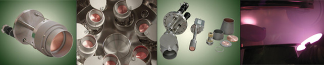
MODULAR MAGNET ARRAY - MAGNETRON SPUTTER SOURCE
A modular magnet array is a special magnetron sputtering source feature developed by AJA International, Inc. in 1991 to allow the end user to convert the specific magnetic field of the source to a variety of configurations. For example, each source can be configured to operate in the:
- "Balanced mode" to minimize substrate ion / electron bombardment.
- "Unbalanced mode" to utilizing simultaneous ion bombardment to enhance film properties.
- "Magnetic material mode" to help the magnetic field saturate and overcome the shunting effect of magnetic target materials allowing the magnetron sputter deposition of high permeability targets such as Fe.
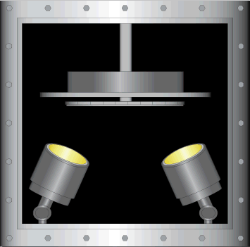
CONFOCAL SPUTTERING

A confocal sputtering system configuration is when multiple magnetron sputtering sources are arranged in a specific circular pattern and are aimed at a common focal point. When a substrate is placed in the vicinity of this focal point and rotated on its own axis, it is possible to deposit highly uniform single layers, multi-layers and co-deposited alloy films. It is an extremely popular technique for the following reasons:
- Exceptional deposition uniformity can be achieved on substrates twice the diameter of the source targets.
- Ability to ea
sily control the growth of successive layers ranging in thicknesses from less than one atomic mono-layer to thousands of Angstroms. - Minimizes time delay between subsequent layers since the substrate does not have to be re-positioned for each layer. In a con-focal multi-layer deposition, every source shutter opens about one second after the previous shutter has closed thereby keeping the deposited film surface on the substrate "in the plasma". This keeps the interface surface free from contamination by residual gas and prevents nucleation of the next layer material.
- Complete freedom to easily grow alloys of any number of materials in any ratio with precise control. This is ideal for combinatorial chemistry applications and for optimization of compound material target stoichiometries for production applications.
- The con-focal sputtering configuration is compact and maintains the substrate holder in an axial orientation. This allows for much more freedom and sophistication in substrate holder design and keeps overall costs down.
- For low deposition rate materials it is possible to boost the rate by running 2-3 targets of this material simultaneously from a single power supply.
IN-SITU TILT SOURCES IN A CONFOCAL SPUTTERING SYSTEM
In powerful R&D sputtering systems with the maximum level of flexibility, end users like to have the ability to operate at different "working distances" (distance between target and substrate). In order to maintain high deposition uniformity, the focal point of the magnetron sputtering sources must be variable by adjusting the source head angle. Also, the deposition profile of materials deposited with DC, with RF and with magnetic materials are all different, so the optimal angle for each material is not identical even if the working distance remains unchanged.
In 1991 AJA International, Inc. invented the world's first UHV and HV magnetron sputter sources withIN-SITU TILT. Without breaking vacuum, each source head angle could be individually set with a precision micrometer to a specific angle. If removed for service or cleaning, it could be returned to the system and set to precisely the same angle - this is much more difficult to accomplish with manually adjustable, source head tilt assemblies. IN-SITU TILT combined with a load-lock on the sputtering system also saves a significant amount of time in performing quick test runs in succession to zero in on the optimal source angles. What can be done in a few hours on a system with load-lock and IN-SITU TILT can take weeks on a system with manual source head tilt since adjustment requires venting the chamber each time to reset the angle. Finally, IN-SITU TILT permits the user to tilt the source away from the substrate and grow "gradient" or "wedge" films which are popular in combinatorial chemistry applications.
DIRECT SPUTTERING
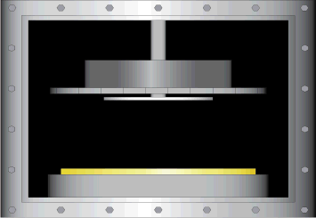
A direct sputtering system configuration is when the substrate is positioned or moving directly in front of and parallel to the magnetron sputtering source targets. As a rule, target diameters (or "lengths" as in the case of rectangular magnetron sputtering sources) should be about 20% to 30% larger than the substrate to achieve reasonable uniformity. For example a 100 mm wafer would require a 150 mm sputter target to achieve +/- 5% deposition uniformity. Although this configuration is much less flexible and generally more expensive than con-focal sputtering, it has its place in production applications which require maximum deposition rates (semiconductor wafer metallization), applications which utilize large substrates (e.g. flat panel displays) and a few techniques that demand "line-of-sight deposition" (e.g. "lift-off").
Utilizing a direct sputtering configuration for R&D is justified in certain instances, but often is chosen because it is what the researcher has "seen before". Like diode sputtering, this was the original sputter system configuration and "old habits die hard". It is important to clearly evaluate your needs before choosing between direct and con-focal deposition orientation.
AJA - THE CUTTING EDGE IN SPUTTERING TECHNOLOGY
스퍼터링 기술의 최첨단- AJA International
고품질의 혁신적인 디자인과 product flexibility, 고객 지원, 적절한 가격에 초점을 맞춘 AJA International는 R&D 스퍼터링 장비 분야에서 명실상부한 리더입니다. 이 회사는 1989 년 창립 이래 시장을 계속 주도함으로써 "pushed the envelope"- 한계를 초월했습니다. AJA의 디자인은 벤치마킹되지만, 결코 동등하지 않습니다.

검색 결과 4건
- 분류 : Vacuum Deposition System
| 카테고리 | 제목 | 작성자 | 조회수 | |
|---|---|---|---|---|
| E-BEAM EVAPORATION | TUTORIALS FOR ELECTRON BEAM (E-BEAM) EVAPORATION file | YEONJIN | 1383 | TUTORIALS FOR ELECTRON BEAM (E-BEAM) EVAPORATION file |
| ION MILLING | WHAT IS ION MILLING? file | YEONJIN | 1532 | WHAT IS ION MILLING? file |
| SPUTTERING | WHAT IS SPUTTERING? file | YEONJIN | 1276 | WHAT IS SPUTTERING? file |
| THERMAL EVAPORATION | TUTORIALS FOR THERMAL EVAPORATION file | YEONJIN | 1247 | TUTORIALS FOR THERMAL EVAPORATION file |