

Pyrolytic Graphite Crucible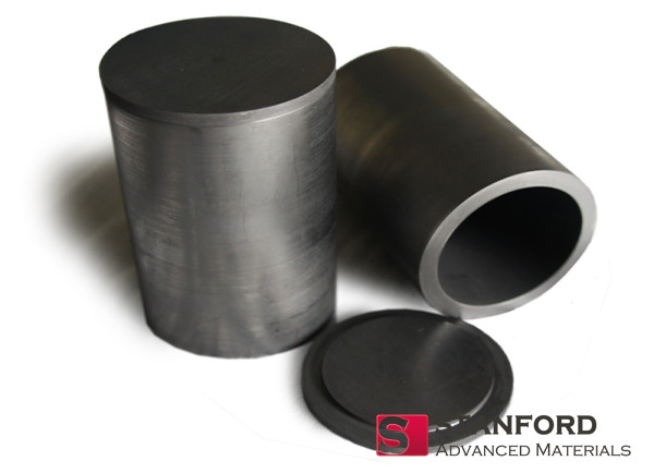
|
Catalog No. |
GR0191 |
|---|---|
|
Size |
Various |
|
Material |
Pure pyrolytic graphite |
|
Purity |
99% |
|
Shape |
Crucible |
Stanford Advanced Materials (SAM) provides pyrolytic graphite crucible of coated and whole types. We can supply 1~200ml crucibles for whole pyrolytic graphite material and larger sizes are available for coated products. The largest available size for PG coated products can be 350mm*600mm.
Product Overview
Our pyrolytic graphite (PG) crucibles represent the pinnacle of high-temperature containment solutions, engineered for the most demanding metallurgical and semiconductor applications. Manufactured through advanced chemical vapor deposition (CVD) technology, these crucibles deliver unmatched purity and performance in high-value material processing.
Key Features & Benefits
1. Ultra-High Purity Construction
-
CVD process using 99.999% pure methane feedstock
-
Total impurities <10ppm (vs. 100-500ppm in conventional graphite)
-
Ideal for semiconductor crystal growth and high-purity metal evaporation
2. Superior Thermal Performance
-
Continuous operation up to 2300°C (in inert/vacuum)
-
Thermal conductivity: 400-1500 W/m·K (anisotropic)
-
Exceptional thermal shock resistance (ΔT >1500°C)
3. Advanced Material Properties
-
Bulk density: 2.10-2.23 g/cm³
-
Flexural strength: 70-120 MPa
-
Near-zero porosity (<0.5% vs. 10-15% in standard graphite)
4. Custom Engineering Options
-
Available as pure CVD or graphite-substrate coated versions
-
Standard wall thickness: 1mm (custom 0.5-5mm available)
-
Optional silicon carbide coating for enhanced oxidation resistance
Pyrolytic Graphite Crucible Technical Specifications
|
Parameter |
Specification |
|---|---|
|
Material Type |
Pyrolytic Graphite (PG) |
|
Manufacturing Process |
Chemical Vapor Deposition (CVD) |
|
Carbon Content |
99.999% |
|
Maximum Operating Temp |
2300°C (inert/vacuum) |
|
Thermal Conductivity |
400-1500 W/m·K (in-plane) |
|
Density |
2.10-2.23 g/cm³ |
|
Porosity |
<0.5% |
|
Standard Coating Thickness |
30μm (custom 10-500μm) |
|
Lead Time |
3-4 weeks (standard) |
Application Scenarios
Semiconductor Manufacturing
-
MBE and MOCVD systems
-
GaAs, GaN crystal growth
-
Silicon carbide processing
Specialty Metallurgy
-
Ultra-high purity metal evaporation (Al, Au, Ag)
-
Titanium and platinum group metal processing
-
Rare earth element refining
Research & Development
-
High-temperature material studies
-
Thin film deposition systems
-
Advanced battery material development
Contact Our Experts
Have specific application requirements? Our materials engineers are ready to assist with:
-
Material selection guidance
-
Custom design consultation
-
Process optimization advice
-
Technical documentation