Different Types of Evaporation Materials
(주)연진에스텍은 Granule, Beads & Sphere, Lump, Rod, Powder, Single Crystal 등 대부분의 Evaporation Process에 부합하는 다양한 형태의 증발 증착물질을 제공합니다.
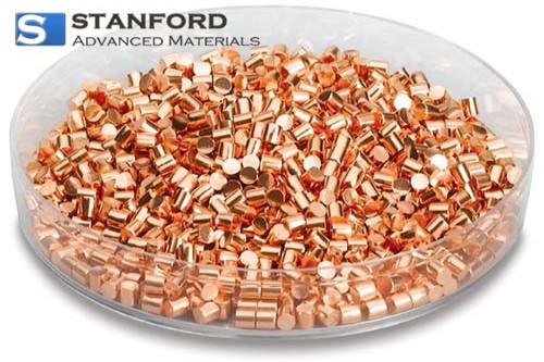
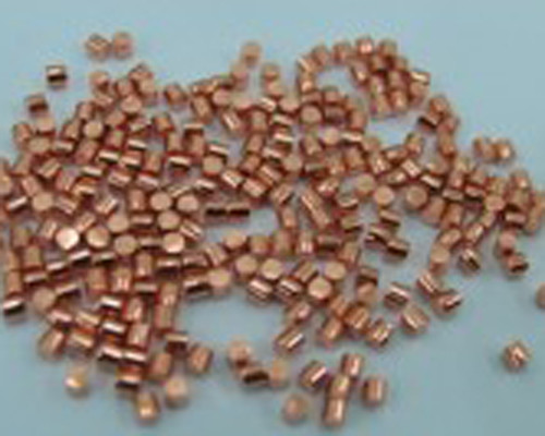
Copper (Cu) Evaporation Materials
Description:
Copper Evaporation Materials are crucial for thin film deposition processes, possessing distinctive properties suited for various applications. Recognized for their high purity and controlled evaporation rates, they ensure precise film deposition onto substrates, facilitating uniform and defect-free film formation. With exceptional thermal conductivity and electrical conductivity, Copper Evaporation Materials are extensively used in semiconductor devices, integrated circuits, and electrical contacts. Additionally, they find applications in decorative coatings, where they provide a lustrous finish. Versatile and reliable, Copper Evaporation Materials play a vital role in industries requiring thin film fabrication, offering consistent performance and enabling technological advancements.
Copper (Cu) Evaporation Materials Specification:
|
Material |
Copper |
|
Appearance |
Copper, Metallic |
|
Melting Point (°C) |
1,083 |
|
Thermal Conductivity |
400W/m.K |
|
Coefficient of Thermal Expansion |
16.5 x 10⁻⁶/K |
|
Theoretical Density (g/cc) |
8.92 |
Copper (Cu) Evaporation Materials Applications:
1. Semiconductor devices: metallic, conductive and connecting layers for the preparation of semiconductor devices, e.g., in integrated circuits, transistors and solar cells.
2. Integrated circuits: Materials used as metallic connecting wires and electrodes for the preparation of semiconductor devices and electronic components.
3. Electronics: Conductive layers and electrodes for the preparation of electronic devices, e.g., resistors, capacitors, and sensors.
4. Decorative coatings: Materials used as decorative coatings to give surfaces a metallic sheen and color, e.g., in jewelry, sculptures and works of art.
5. Thermally conductive materials: Due to their excellent thermal conductivity, copper is also used as a component of heat sinks and thermally conductive materials, e.g., in electronic, automotive, and industrial equipment.
Copper (Cu) Evaporation Materials Packaging:
Our evaporation materials are carefully handled to prevent damage during storage and transportation and to preserve the quality of our products in their original condition.
FAQs
Q1: What are Copper Evaporation Materials?
A1: Copper (Cu) evaporation materials are high-purity copper in forms such as pellets, granules, or pieces, used in physical vapor deposition (PVD) processes to create thin films. These films are widely applied in electronics, optics, and decorative coatings.
Q2: What are the main applications of Copper Evaporation Materials?
A2: Copper evaporation materials are commonly used in:
Semiconductor and microelectronics (interconnect layers, conductive films)
Optical coatings (reflective and conductive layers)
Thin-film solar cells (Cu-based absorber layers)
Decorative coatings (aesthetic finishes in luxury products)
Aerospace and automotive industries (functional coatings for durability and conductivity)
Q3: Which deposition techniques are compatible with Copper Evaporation Materials?
A3: Copper can be deposited using:
Electron beam (E-beam) evaporation – Provides precise and uniform film deposition.
Thermal evaporation – Suitable for lower-cost applications.
Sputtering – An alternative PVD method for high-performance coatings.

- High Purity & Performance 일관된 증착 품질과 오염을 줄이도록 가공합니다.
- Material Variety 다양한 응용 분야의 요구 사항에 맞게 순수 금속, 합금, 세라믹 및 화합물로 제공됩니다.
- Custom Manufacturing 특정 시스템의 필요요구 사항에 맞게 크기와 형태, 조성을 맞춤화했습니다.
- Precision Design 반복 가능하고 균일한 박막 결과를 위해 엄격한 공차로 제조되었습니다.
- Flexible Supply Chain 최고의 제조업체와 강력한 파트너십을 통해 일관된 품질과 on-time 납품을 보장합니다.