Different Shapes of Sputtering Targets
(주)연진에스텍은 Planar (flat) Target과 Rotary (cylindrical) Target, Circular Target 및 Ring Target 등 대부분의 증착 공정에 부합하는 다양한 형태의 스퍼터링 타겟을 제공하며, 타겟 크기의 커스터마이즈가 가능합니다.
- High Purity & Performance 일관된 증착 품질과 오염을 줄이도록 가공합니다.
- Material Variety 다양한 응용 분야의 요구 사항에 맞게 순수 금속, 합금, 세라믹 및 화합물로 제공됩니다.
- Custom Manufacturing 특정 시스템의 필요요구 사항에 맞게 크기와 형태, 조성을 맞춤화했습니다.
- Precision Design 반복 가능하고 균일한 박막 결과를 위해 엄격한 공차로 제조되었습니다.
- Flexible Supply Chain 최고의 제조업체와 강력한 파트너십을 통해 일관된 품질과 on-time 납품을 보장합니다.
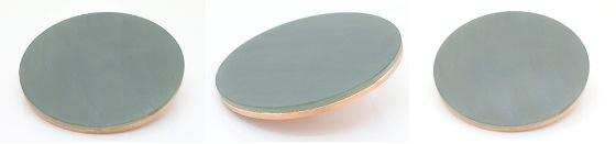
Silicon Dioxide Sputtering Target, SiO2

High-Purity SiO2 Sputtering Target for Advanced Thin Film Applications
Silicon Dioxide Sputtering Target Description
Silicon dioxide sputtering target from Stanford Advanced Materials contains Si and O. Silicon dioxide (SiO2), also known as Silica, is a natural compound made from two of the most abundant materials on the planet: silicon (Si) and oxygen (O2). Silica is most commonly considered to be in the form of quartz. It exists naturally in water, plants, animals and the earth. 59% of the earth’s crust is composed of silicon dioxide. In addition, it also forms more than 95% of the known rocks on Earth. Here is the structure of SiO2.

Silicon Dioxide Sputtering Target Chemical Structure
Key Features:
- High purity options: 99.9% to 99.995%
- Available shapes: discs, rectangles, tubes
- Sizes ranging from 1” to over 20” diameter or custom dimensions
- Thickness typically from 0.0625” to 0.25”
- Bonding options: indium, elastomer, or unbonded
- High melting point (~1600°C) and density (~2.53 g/cm³)
- Excellent optical transparency and dielectric properties
- Vacuum or sealed packaging to prevent moisture and damage
Silicon Dioxide Sputtering Target Specification
|
Material Type |
Silicon (IV) Oxide |
|
Symbol |
SiO2 |
|
Color/Appearance |
White, Crystalline Solid |
|
Melting Point (°C) |
1,610 |
|
Boiling Point (°C) |
2,230 |
|
Density (kg/m-3) |
2,533 |
|
Sputter |
RF |
|
Type of Bond |
Copper, Indium, Elastomer |
|
Comments |
Quartz is excellent in E-beam. |
|
Available Sizes |
Dia.: 1.0″, 2.0″, 3.0″, 4.0″, 5.0″, 6.0″ |
We also offer other customized shapes and sizes of the sputtering targets. Please send us an inquiry for more information.
Silicon Dioxide Sputtering Target Applications
- Semiconductor Industry:
Used to deposit high-quality dielectric layers in integrated circuits, transistors, and sensors, providing excellent electrical insulation and reliability for advanced semiconductor devices. - Chemical Vapor Deposition (CVD):
Essential for creating uniform, high-purity SiO₂ thin films on various substrates in semiconductor, solar, and aerospace industries, ensuring precise control over film thickness and composition. - Optical Coatings:
Applied in optical devices and displays for transparent, durable coatings that enhance performance and protect surfaces. - Solar Cells and Photovoltaics:
Used to produce protective and functional thin films that improve solar cell efficiency and longevity. - Glass Coatings:
Coatings for automotive and architectural glass to enhance durability, corrosion resistance, and optical clarity.
Silicon Dioxide Sputtering Target Bonding Service
SiO2 sputtering materials are commonly available with indium bonding and elastomer bonding options. Copper bonding is also widely used and can be customized based on customer requirements. Stanford Advanced Materials specializes in machining standard backing plates and collaborates with Taiwan Bonding Company to provide comprehensive bonding services. For inquiries about target bonding materials, methods, and services, please click here.
Packaging
Our silicon oxide sputtering targets are tagged and labeled externally for efficient identification and quality control. They are vacuum-packed to prevent moisture absorption and carefully cushioned to avoid damage during storage and transportation.
Get Contact
High-quality silicon dioxide sputtering targets are available in various forms, purities, sizes, and prices. We specialize in producing high-purity thin film coating materials with the highest possible density and smallest possible average grain sizes for use in semiconductor, chemical vapor deposition (CVD), and physical vapor deposition (PVD) display and optical applications. Please send us an inquiry for current pricing on sputtering targets and other deposition materials not listed.
FAQs of Silicon Dioxide Sputtering Target
Q1: What purity levels are available for silicon dioxide sputtering targets?
Purity levels typically range from 99.9% to 99.995%, ensuring high-quality thin films.
Q2: How is the silicon dioxide sputtering target packaged?
Targets are vacuum-sealed or moisture-proof packed to protect against damage and contamination.
Q3: Can silicon dioxide sputtering targets be customized?
Yes, sizes, shapes, and bonding types can be tailored to meet specific application needs.
Q4: Can SiO₂ be deposited using DC sputtering?
Not ideal. SiO₂ is a dielectric, so it tends to accumulate charge under DC sputtering. RF sputtering is the better option for stable, uniform growth.
Q5. Can SiO₂ form epitaxial films? On what substrates?
Yes, under the right conditions. Compatible substrates include silicon (Si), gallium arsenide (GaAs), aluminum (Al), and gallium nitride (GaN).
Q6. Where are SiO₂ thin films used?
They show up in everything from semiconductors and solar cells to optical lenses, displays, drug delivery systems, implants, and data storage like CDs and DVDs.

하기