Different Shapes of Sputtering Targets
(주)연진에스텍은 Planar (flat) Target과 Rotary (cylindrical) Target, Circular Target 및 Ring Target 등 대부분의 증착 공정에 부합하는 다양한 형태의 스퍼터링 타겟을 제공하며, 타겟 크기의 커스터마이즈가 가능합니다.
- High Purity & Performance 일관된 증착 품질과 오염을 줄이도록 가공합니다.
- Material Variety 다양한 응용 분야의 요구 사항에 맞게 순수 금속, 합금, 세라믹 및 화합물로 제공됩니다.
- Custom Manufacturing 특정 시스템의 필요요구 사항에 맞게 크기와 형태, 조성을 맞춤화했습니다.
- Precision Design 반복 가능하고 균일한 박막 결과를 위해 엄격한 공차로 제조되었습니다.
- Flexible Supply Chain 최고의 제조업체와 강력한 파트너십을 통해 일관된 품질과 on-time 납품을 보장합니다.
Lead Arsenide Sputtering Target, PbAs
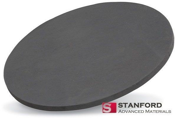
Lead Arsenide Sputtering Target
Description
Lead Arsenide Sputtering Targets find application in sputter deposition processes, facilitating the preparation of thin films for use in electronics, optoelectronics, and various semiconductor applications. These sputtering targets consist of semiconducting materials, showcasing conductivity levels between that of a conductor and an insulator. This unique property positions the Lead Arsenide Sputtering Target as a promising material for the preparation of semiconductor devices.
With a direct energy gap, Lead Arsenide requires relatively small amounts of energy for electron and hole transitions. This characteristic makes Lead Arsenide potentially advantageous in the creation of optoelectronic devices, where efficient energy transitions are crucial. Additionally, Lead Arsenide Sputtering Targets typically exhibit relatively good thermal stability, allowing for application in high-temperature scenarios within specified limits.
Lead Arsenide Sputtering Target Specifications
|
Compound Formula |
PbAs |
|
Molecular Weight |
282.12 |
|
Appearance |
Grey Target |
|
Available Sizes |
Dia.: 1.0″, 2.0″, 3.0″, 4.0″, 5.0″, 6.0″
Thick: 0.125″, 0.250″ |
Lead Arsenide Sputtering Target Handling Notes
- Indium bonding is recommended for Lead Arsenide Sputtering Targets, due to some of its characteristics not amenable to sputtering like brittleness, low thermal conductivity, etc.
- This material has a low thermal conductivity and is susceptible to thermal shock.
Lead Arsenide Sputtering Target Application
- Semiconductor device preparation: Lead Arsenide Sputtering Targets can be used for sputtering deposition for the preparation of semiconductor devices such as thin film transistors (TFTs) and other integrated circuit components.
- Optoelectronics devices: Since Lead Arsenide (PbAs) is a semiconductor material, Lead Arsenide Sputtering Targets can be used to prepare devices for applications in optoelectronics, such as photodetectors and lasers. In addition, the application of Lead Arsenide Sputtering Targets involves the preparation of semiconductor nanostructures such as nanowires and nanodots, which are used in the research and development of new nanoelectronics devices.
- Topological insulator research: In some cases, Lead Arsenide (PbAs) may exhibit topological insulator properties, so Lead Arsenide Sputtering Targets may be used for research in topological physics.
Lead Arsenide Sputtering Target Packaging
Our Lead Arsenide Sputtering Target is carefully handled during storage and transportation to preserve the quality of our products in their original condition.

하기