Different Shapes of Sputtering Targets
(주)연진에스텍은 Planar (flat) Target과 Rotary (cylindrical) Target, Circular Target 및 Ring Target 등 대부분의 증착 공정에 부합하는 다양한 형태의 스퍼터링 타겟을 제공하며, 타겟 크기의 커스터마이즈가 가능합니다.
- High Purity & Performance 일관된 증착 품질과 오염을 줄이도록 가공합니다.
- Material Variety 다양한 응용 분야의 요구 사항에 맞게 순수 금속, 합금, 세라믹 및 화합물로 제공됩니다.
- Custom Manufacturing 특정 시스템의 필요요구 사항에 맞게 크기와 형태, 조성을 맞춤화했습니다.
- Precision Design 반복 가능하고 균일한 박막 결과를 위해 엄격한 공차로 제조되었습니다.
- Flexible Supply Chain 최고의 제조업체와 강력한 파트너십을 통해 일관된 품질과 on-time 납품을 보장합니다.
Cadmium Arsenide Sputtering Target, Cd3As2
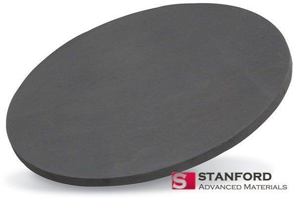
Cadmium Arsenide Sputtering Target
Description
Cadmium Arsenide Sputtering Targets are made of high-purity Cadmium Arsenide (Cd3As2), with a wide range of purity grades and morphology sizes to choose from under high-quality assurance, which can be applied to a variety of research and production needs. It can be used in chemical vapor deposition (CVD) and physical vapor deposition (PVD) to produce thin films, and under the quality assurance of the target, uniform and extremely thin film coverage can be obtained. Cadmium Arsenide (Cd3As2) itself has some unique properties that determine its unique application scenarios. Cadmium Arsenide (Cd3As2) exhibits semiconducting properties, which can be used in related semiconductor device fabrication. Cadmium Arsenide (Cd3As2) is considered to be a three-dimensional topological insulator, and its topological properties make it unique potential for applications in several topological insulators and topological insulator materials. In addition, in the field of magnetism, the crystal structure of Cadmium Arsenide (Cd3As2) may cause it to exhibit antimagnetic properties, which is of some importance in the study of magnetic materials and possible applications.
Cadmium Arsenide Sputtering Target Specifications
|
Compound Formula |
Cd3As2 |
|
Molecular Weight |
487.08 |
|
Appearance |
Grey Target |
|
Melting Point |
716℃ |
|
Density |
3.031 g/cm3 |
|
Available Sizes |
Dia.: 1.0″, 2.0″, 3.0″, 4.0″, 5.0″, 6.0″
Thick: 0.125″, 0.250″ |
Cadmium Arsenide Sputtering Target Handling Notes
- Indium bonding is recommended for Cadmium Arsenide Sputtering Target, due to some of its characteristics not amenable to sputtering like brittleness, low thermal conductivity, etc.
- This material has a low thermal conductivity and is susceptible to thermal shock.
Cadmium Arsenide Sputtering Target Application
- Thin Film Deposition: Cadmium Arsenide Sputtering Targets can be employed in physical vapor deposition (PVD) or chemical vapor deposition (CVD), where sputter deposition is utilized. By placing Cadmium Arsenide Sputtering Targets in a vacuum chamber and using high-energy ions or electrons to bombard the target, thin films can be generated for the fabrication of semiconductor devices.
- Semiconductor Device Fabrication: Thin films of Cadmium Arsenide (Cd3As2) can be used in the fabrication of semiconductor devices, including thin-film transistors, photodiodes, and other electronic and optoelectronic devices. Sputter-deposited films find applications in the semiconductor industry.
- Magnetic Material Research: Due to the potential for Cadmium Arsenide (Cd3As2) to exhibit antiferromagnetic properties based on its crystal structure, sputter deposition of Cadmium Arsenide Sputtering Targets can be applied in the research and preparation of magnetic materials.
Cadmium Arsenide Sputtering Target Packaging
Our Cadmium Arsenide Sputtering Target is carefully handled during storage and transportation to preserve the quality of our products in their original condition.

하기