Different Shapes of Sputtering Targets
(주)연진에스텍은 Planar (flat) Target과 Rotary (cylindrical) Target, Circular Target 및 Ring Target 등 대부분의 증착 공정에 부합하는 다양한 형태의 스퍼터링 타겟을 제공하며, 타겟 크기의 커스터마이즈가 가능합니다.
Cryolite Sputtering Target, Na3·AlF6
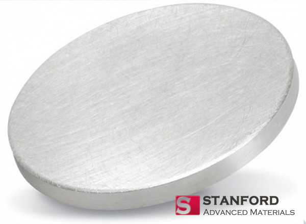
Cryolite Sputtering Target
Description
Cryolite Sputtering Target is a material used in the sputtering process for depositing thin films onto substrates. Cryolite is a mineral compound consisting of sodium (Na), aluminum (Al), and fluorine (F) ions. In sputtering, high-energy ions are directed at the cryolite sputtering target, causing atoms or molecules to be ejected from the target surface. These ejected particles then deposit onto a substrate, forming a thin film with properties inherited from the cryolite material.
Cryolite Sputtering Target Specifications
|
Compound Formula |
Na3·AlF6 |
|
Molecular Weight |
209.94 |
|
Appearance |
Gray target |
|
Melting Point (℃) |
950-1012 |
|
Density (g/cm3) |
2.9-3.0 |
|
Available Sizes |
Dia.: 1.0″, 2.0″, 3.0″, 4.0″, 5.0″, 6.0″
Thick: 0.125″, 0.250″ |
Cryolite Sputtering Target Handling Notes
- Indium bonding is recommended for Cryolite Sputtering Target, due to some of its characteristics not amenable to sputtering like brittleness, low thermal conductivity, etc.
- This material has a low thermal conductivity and is susceptible to thermal shock.
Cryolite Sputtering Target Application
- Optical Coatings: Cryolite thin films can be used in optical coatings for various applications, such as anti-reflective coatings and interference filters.
- Semiconductor Manufacturing: Cryolite coatings may find applications in the semiconductor industry, particularly in the fabrication of electronic and optoelectronic devices.
- Research and Development: Cryolite thin films may be used in research and development for specific applications where the properties of cryolite are desirable.
Cryolite Sputtering Target Packaging
Our Cryolite Sputtering Target is widely used in the production of coatings for various purposes, such as improving the wear resistance of tools, enhancing the durability of surfaces, or providing specific optical or electrical properties.

- High Purity & Performance 일관된 증착 품질과 오염을 줄이도록 가공합니다.
- Material Variety 다양한 응용 분야의 요구 사항에 맞게 순수 금속, 합금, 세라믹 및 화합물로 제공됩니다.
- Custom Manufacturing 특정 시스템의 필요요구 사항에 맞게 크기와 형태, 조성을 맞춤화했습니다.
- Precision Design 반복 가능하고 균일한 박막 결과를 위해 엄격한 공차로 제조되었습니다.
- Flexible Supply Chain 최고의 제조업체와 강력한 파트너십을 통해 일관된 품질과 on-time 납품을 보장합니다.