Different Shapes of Sputtering Targets
(주)연진에스텍은 Planar (flat) Target과 Rotary (cylindrical) Target, Circular Target 및 Ring Target 등 대부분의 증착 공정에 부합하는 다양한 형태의 스퍼터링 타겟을 제공하며, 타겟 크기의 커스터마이즈가 가능합니다.
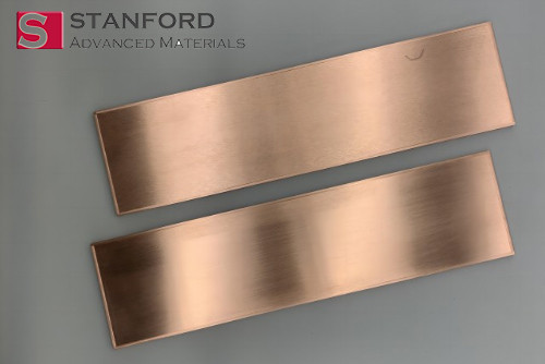
Aluminum Tin Copper Planar Target (AlSnCu Planar Target)
Overview of Aluminum Tin Copper Planar Target (AlSnCu Planar Target)
The AlSnCu Planar Target is a sophisticated ternary alloy designed for reliable and efficient sputtering operations. It combines the lightweight and corrosion-resistant properties of aluminum with the superior electrical and thermal conductivity of copper and the enhanced lubricity and malleability provided by tin. This alloy ensures excellent film uniformity through its consistent microstructure, achieved via precise alloying and controlled solidification methods. It offers strong adhesion, balanced hardness, and a lower melting point, ensuring compatibility with a diverse range of substrate materials. The presence of tin minimizes sputtering-related defects and boosts process stability, while copper guarantees uniform conductivity across the deposited films. Its balanced thermal expansion makes it suitable for integration with substrates sensitive to temperature variations, and it performs reliably in both DC and RF sputtering environments.
Specifications of Aluminum Tin Copper Planar Target (AlSnCu Planar Target)
Chemical Composition: Al, Sn, Cu
Purity: 99.9%
Shape: Planar
Note: The specifications provided are based on theoretical data. For tailored requirements and detailed information, please reach out to us.
Custom Dimensions
- Thickness: 3 mm ± 0.5 mm (customizable)
- Diameter: 50 mm ± 1 mm (customizable)
Applications of Aluminum Tin Copper Planar Target (AlSnCu Planar Target)
-
Semiconductor Interconnects: Utilized for depositing conductive layers in microelectronic devices, enhancing adhesion and reliability. Aluminum reduces weight, copper increases conductivity, and tin improves solderability.
-
Display Technologies: Employed in thin-film transistors (TFTs) and interconnects for LCD and OLED displays, ensuring excellent patterning and uniform surface coatings.
-
Flexible Electronics: Suitable for wearable or bendable electronic circuits due to its ductility and strong bonding with polymer substrates.
-
Printed Circuit Boards (PCBs): Used in sputtering processes for metallization layers in high-density PCBs, providing robust mechanical bonding and effective thermal management.
-
Automotive Electronics: Ideal for sensor modules and control units operating in demanding environments, offering resistance to oxidation and thermal cycling.
-
Energy Storage Devices: Applied in advanced battery and capacitor technologies as current collectors or electrode films that require low mass and high conductivity.
Packaging Options for Aluminum Tin Copper Planar Target (AlSnCu Planar Target)
Our AlSnCu Planar Targets are packaged to ensure their safety during transit. Depending on the size and dimensions, smaller targets are securely housed in polypropylene (PP) boxes, while larger ones are shipped in custom-built wooden crates. We prioritize customized packaging solutions and utilize appropriate cushioning materials to provide maximum protection during transportation.
Packaging Choices:
- Carton
- Wooden Box
- Custom Packaging
Manufacturing Process
Manufacturing Process Overview

Testing Methods
- Chemical Composition Analysis: Utilizes methods such as Glow Discharge Mass Spectrometry (GDMS) or X-Ray Fluorescence (XRF) to confirm purity and composition.
- Mechanical Properties Testing: Assesses tensile strength, yield strength, and elongation to evaluate material performance.
- Dimensional Inspection: Measures thickness, width, and length to ensure they meet specified tolerances.
- Surface Quality Inspection: Detects defects like scratches, cracks, or inclusions through visual and ultrasonic examinations.
- Hardness Testing: Determines material hardness to ensure uniformity and mechanical reliability.
Frequently Asked Questions about Aluminum Tin Copper Planar Target (AlSnCu Planar Target)
Q1: What purity levels are available?
A1: SAM offers AlSnCu targets with purities of ≥99.99%, ideal for high-precision thin film deposition applications.
Q2: Is this target compatible with both DC and RF sputtering systems?
A2: Yes, AlSnCu targets are suitable for both DC and RF sputtering processes, depending on your specific equipment and film requirements.
Q3: What sputtering conditions are recommended?
A3: High-purity argon is typically used as the working gas. Sputtering power, pressure, and temperature settings should be optimized based on the chamber design and target size.
Performance Comparison: AlSnCu Target vs. Cu Target vs. AlSi Target
|
Property |
AlSnCu Target |
Cu Target |
AlSi Target |
|---|---|---|---|
|
Composition |
Al + Sn + Cu |
Pure Cu |
Al + Si |
|
Magnetic Properties |
Non-magnetic |
Non-magnetic |
Non-magnetic |
|
Corrosion Resistance |
Good |
Excellent |
Good |
|
Thermal Stability |
Moderate |
High |
Moderate |
|
Wear Resistance |
Good |
Moderate |
Moderate |
|
Electrical Conductivity |
Moderate |
Excellent |
Moderate |
|
Density |
~7.3 g/cm³ |
~8.96 g/cm³ |
~2.7 g/cm³ |
|
Melting Point |
~230°C – 280°C |
~1,085°C |
~577°C |
|
Applications |
Electronics, coatings, batteries |
Conductors, electronics, coatings |
Semiconductors, solar cells, coatings |
Additional Information
Raw Materials – Aluminum
Physical Properties:
- Density: 2.7 g/cm³
- Melting Point: ~660°C
- Structure: Face-centered cubic (FCC)
- Magnetic: Non-magnetic
Chemical Properties:
- Forms a natural oxide layer that prevents further oxidation
- Exhibits excellent thermal and electrical conductivity
- Highly ductile and easily alloyed with other metals
Industrial Applications:
- Structural Components: Used extensively in aerospace, automotive, and construction for its lightweight and strength.
- Electrical Applications: Essential in electrical wiring and heat exchangers due to its high conductivity.
- Thin Film Technologies: Provides a lightweight and corrosion-resistant base for various sputtering applications.
Raw Materials – Tin
Physical Properties:
- Density: 7.31 g/cm³
- Melting Point: 231.9°C
- Structure: Metallic, grayish appearance
- Electrical Conductivity: Good
Chemical Properties:
- Highly resistant to corrosion, especially from water and acidic environments
- Forms strong bonds with other metals, enhancing alloy properties
- Exhibits excellent lubricity and solderability
Industrial Applications:
- Surface Coatings: Used to prevent corrosion and improve lubrication.
- Alloying Agent: Enhances the mechanical properties of metals, improving strength and durability.
- Thin Films: Contributes to improved ductility and wetting behavior in sputtered films.
Raw Materials – Copper
Physical Properties:
- Density: ~8.96 g/cm³
- Melting Point: ~1,085°C
- Structure: Face-centered cubic (FCC)
- Electrical Conductivity: Excellent
Chemical Properties:
- Highly resistant to corrosion in various environments
- Easily alloyed with other metals to enhance mechanical properties without significantly reducing conductivity
- Forms a natural patina that protects against further oxidation
Industrial Applications:
- Electrical Wiring: Predominantly used for electrical conductors due to its superior conductivity.
- Thermal Management: Utilized in heat sinks and exchangers for efficient heat dissipation.
- Metallization Processes: Essential in creating conductive layers in electronics and thin film technologies.

- High Purity & Performance 일관된 증착 품질과 오염을 줄이도록 가공합니다.
- Material Variety 다양한 응용 분야의 요구 사항에 맞게 순수 금속, 합금, 세라믹 및 화합물로 제공됩니다.
- Custom Manufacturing 특정 시스템의 필요요구 사항에 맞게 크기와 형태, 조성을 맞춤화했습니다.
- Precision Design 반복 가능하고 균일한 박막 결과를 위해 엄격한 공차로 제조되었습니다.
- Flexible Supply Chain 최고의 제조업체와 강력한 파트너십을 통해 일관된 품질과 on-time 납품을 보장합니다.