Different Shapes of Sputtering Targets
(주)연진에스텍은 Planar (flat) Target과 Rotary (cylindrical) Target, Circular Target 및 Ring Target 등 대부분의 증착 공정에 부합하는 다양한 형태의 스퍼터링 타겟을 제공하며, 타겟 크기의 커스터마이즈가 가능합니다.
Overview of Niobium Tin Target (NbSn Target)
The NbSn Target is a binary alloy designed for sputtering processes, offering a distinctive blend of superconducting, structural, and electrical attributes. Niobium contributes exceptional mechanical strength, a high melting point, and chemical stability, while tin enhances ductility and supports the formation of superconducting intermetallic compounds like NbSn. This target ensures excellent thermal conductivity and reliable performance under high-vacuum and high-energy sputtering conditions. Its finely tuned, homogeneous microstructure—achieved through precise alloying and controlled fabrication methods—guarantees consistent film deposition and uniform composition. The NbSn Target exhibits strong adhesion and compatibility with various substrates, supporting a wide array of thin film deposition techniques. This makes it particularly suitable for producing high-purity superconducting layers, conductive coatings, and functional electronic materials.
Specifications of Niobium Tin Target (NbSn Target)
Material Composition: Nb, Sn
Purity: 99.95%
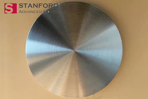
Shape: Planar Disc
Please note that the specifications provided are based on theoretical data. For customized specifications and detailed inquiries, please contact us directly.
Custom Dimensions
- Diameter: Customizable to specific requirements
- Thickness: Adjustable based on application needs
Applications of Niobium Tin Target (NbSn Target)
-
Superconducting Films: Ideal for depositing NbSn thin films used in superconducting magnets, quantum computing components, and cryogenic electronics due to their high critical current density and strong tolerance to magnetic fields.
-
Microelectronics: Utilized in the production of conductive interconnects and barrier layers in microelectronic devices where both structural integrity and electron mobility are essential.
-
MEMS & Sensors: Applied in micro-electro-mechanical systems (MEMS) and sensitive thin-film sensors that require stable, low-resistance metallic coatings.
-
Advanced Coatings: Suitable for high-vacuum and high-temperature coatings in scientific instruments or aerospace-grade electronics.
-
Superconducting RF Cavities: Used in thin-film coatings for accelerator cavities in particle physics research, leveraging the superconducting properties of Nb-Sn compounds.
Packaging Options for Niobium Tin Target (NbSn Target)
Our NbSn Targets are meticulously packaged to ensure safety during transit. Depending on the size and dimensions, smaller targets are securely placed in polypropylene (PP) boxes, while larger ones are shipped in custom-built wooden crates. We prioritize tailored packaging solutions and use appropriate cushioning materials to provide maximum protection during transportation.
Packaging Options:
- Carton
- Wooden Crate
- Custom Packaging
Manufacturing Process

Testing Methods
- Chemical Composition Analysis: Utilizes techniques such as Glow Discharge Mass Spectrometry (GDMS) or X-Ray Fluorescence (XRF) to verify purity and composition.
- Mechanical Properties Testing: Assesses tensile strength, yield strength, and elongation to evaluate material performance.
- Dimensional Inspection: Measures thickness, width, and length to ensure compliance with specified tolerances.
- Surface Quality Inspection: Identifies defects like scratches, cracks, or inclusions through visual and ultrasonic examinations.
- Hardness Testing: Determines material hardness to confirm uniformity and mechanical reliability.
Frequently Asked Questions about Niobium Tin Target (NbSn Target)
Q1: What is the purity level of the NbSn Target provided by SAM?
A1: Stanford Advanced Materials typically offers NbSn Targets with purity levels of 99.9% or higher. Custom purities are available upon request.
Q2: Which sputtering methods are compatible with NbSn Targets?
A2: NbSn Targets are compatible with both RF and DC magnetron sputtering systems and can be used in high-vacuum or reactive environments, depending on the desired film characteristics.
Q3: How should NbSn Targets be stored?
A3: Targets should be stored in a dry, controlled environment, preferably in vacuum-sealed packaging to prevent oxidation or contamination.
Performance Comparison: NbSn Target vs. Nb Target vs. Ta Target
|
Property |
NbSn Target |
Niobium (Nb) Target |
Tantalum (Ta) Target |
|---|---|---|---|
|
Material Composition |
Niobium Tin Alloy |
Pure Niobium |
Pure Tantalum |
|
Applications |
Superconductors |
Electronics, Alloys |
Electronics, Alloys |
|
Melting Point |
~2,410°C |
~2,468°C |
~2,996°C |
|
Density (g/cm³) |
8.56 |
8.57 |
16.6 |
|
Conductivity |
Moderate |
High |
Low |
|
Cost |
Higher |
Moderate |
Higher |
|
Hardness |
Moderate |
Moderate |
High |
Additional Information
Raw Materials – Niobium (Nb)
Physical Properties:
- Density: 8.57 g/cm³
- Melting Point: 2,477°C
- Structure: Body-Centered Cubic (BCC)
- Magnetic: Non-magnetic
Chemical Properties:
- Exhibits an exceptionally high melting point, excellent corrosion resistance, and superconducting properties.
- Forms stable oxides and alloys readily with other elements, especially in the production of high-performance materials.
- Ideal for applications requiring strength at elevated temperatures and compatibility with high-purity materials.
Industrial Applications:
- Superconductors: Essential in creating superconducting magnets and electronic components.
- Aerospace Alloys: Enhances strength and durability in aerospace components.
- Advanced Electronics: Used in fabricating high-performance electronic devices.

Raw Materials – Tin (Sn)
Physical Properties:
- Density: 7.31 g/cm³
- Melting Point: 232°C
- Structure: Body-Centered Tetragonal (BCT)
- Magnetic: Non-magnetic
Chemical Properties
- A soft, silvery-white post-transition metal known for its low melting point, malleability, and corrosion resistance.
- Chemically stable in air and water, making it ideal for protective coatings.
- Plays a key role in forming intermetallic compounds, such as Nb₃Sn, which exhibit superconducting properties.
Industrial Applications:
- Energy Storage: Used in soldering and electrical applications due to its conductivity and malleability.
- Chemical Synthesis: Utilized in various chemical reactions and processes.
- Electronics: Employed in modifying electronic properties in thin films and advanced materials research.

- High Purity & Performance 일관된 증착 품질과 오염을 줄이도록 가공합니다.
- Material Variety 다양한 응용 분야의 요구 사항에 맞게 순수 금속, 합금, 세라믹 및 화합물로 제공됩니다.
- Custom Manufacturing 특정 시스템의 필요요구 사항에 맞게 크기와 형태, 조성을 맞춤화했습니다.
- Precision Design 반복 가능하고 균일한 박막 결과를 위해 엄격한 공차로 제조되었습니다.
- Flexible Supply Chain 최고의 제조업체와 강력한 파트너십을 통해 일관된 품질과 on-time 납품을 보장합니다.