미세 유체 장치(microfluidic device)는 장치의 최종 목적에 따라 다양한 재료로 제조할 수 있습니다.
종종 "Lab on a Chip" 장치라고도 불리는이 장치는 운반, 분리, 혼합을 포함한 다양한 공정에 사용되거나 실제로 반응 용기 역할을 할 수 있습니다. 이러한 장치는 세포 및 박테리아 공정, 연료 전지, 광 유체, 반응 화학 등 다양한 응용 분야에서 사용할 수 있습니다.
미세 유체 장치는 일반적으로 유체 혼합을 위한 마이크로 펌프 등의 역할을 하도록 결합하는 channel과 well로 구성된 구조를 가지고 있습니다. 채널의 치수는 일반적으로 너비가 100 마이크론 미만이고 깊이가 100 마이크론 미만입니다.
이러한 장치는glass을 비롯한, 보로 실리케이트, 폴리머 (예 : PMMA) 등 다양한 재료로 만들 수 있습니다.
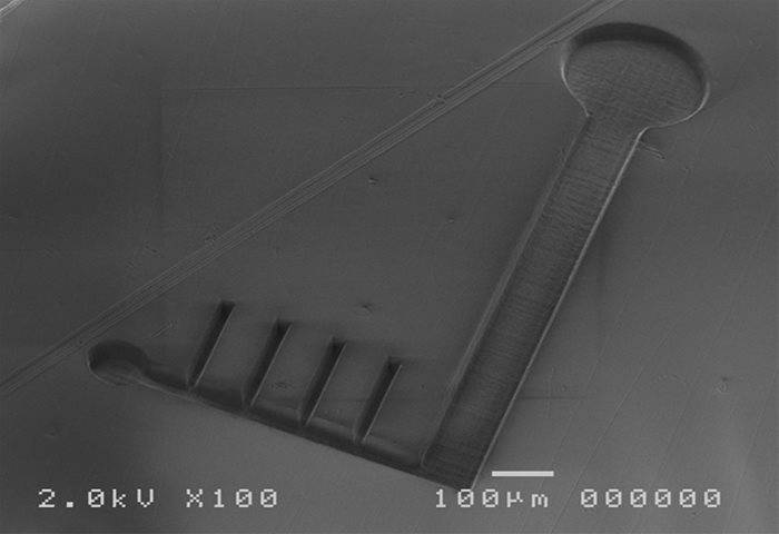
Direct laser ablation은 복잡한 구조를 생성하기 위해 결합될 수있는 구불 구불 한 채널 및 well의 다양한 모양을 생성 할 수 있습니다 (이미지 참조). 또한 기판에 구멍을 만들어 시약을 넣을 수 있습니다.
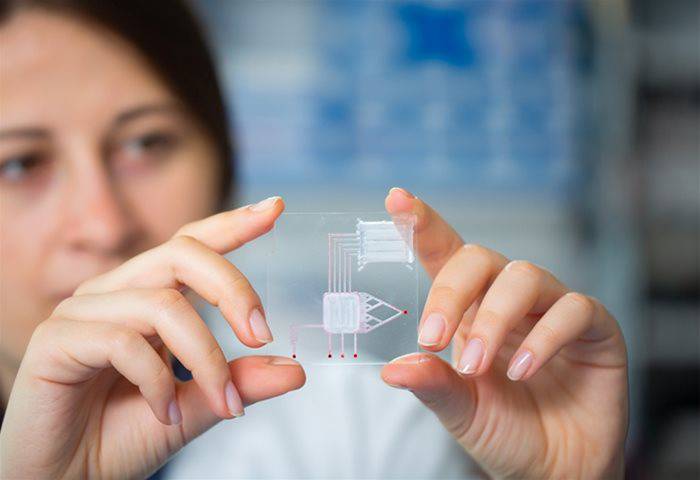
MICROFLUIDICS FOR LAB ON A CHIP DEVICES
Microfluidic devices can be manufactured from a wide variety of material depending on the end purpose of the device.
Often referred to as “Lab on a Chip” devices they can be used for a variety of processes including transport, separation, mixing or indeed act as reaction vessels. Such devices can be used in a variety of applications including cellular and bacterial processes, fuel cells, optofluidics, reaction chemistry etc.
Microfluidic devices typically have structures that are composed of channels and wells, which can be combined to act as micro pumps etc for fluid mixing. Channels have dimensions that are typically < 100 microns wide and 100 microns deep.
These devices can be made form a host of materials including glasses e.g. borosilicate, polymers e.g. PMMA etc.
Direct laser ablation can produce a variety of shapes, see example images, of serpentine channels and wells which can be combined to produced complex structures. In addition, holes in the substrate can be created to allow the introduction of reagents.

하기