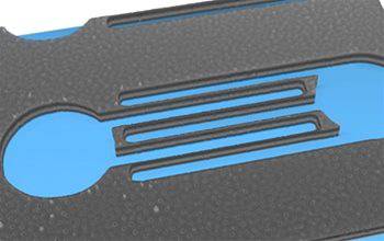
박막 패터닝(thin-film patterning)은 재료 기판에서 단일 또는 여러 레이어를 매우 정밀하게 제거할 수 있는 선택적 레이저 어블레이션 프로세스(selective laser ablation process)입니다.
레이저 박막 패터닝 기술은 기본적으로 laser micro-engraving 또는 각각 레이저 펄스에 의해 소량의 재료를 제거하는 미세 마킹(micro-marking)입니다. 이 과정에서 레이저 빔이 표면 위로 스캔되어 원하는 패턴을 생성합니다. 각 지점에서 펄스 수를 조정하여 마크 또는 패턴의 깊이를 제어 할 수 있습니다.
이 프로세스의 유연성으로 인에 마스크 없이도 다양한 모양과 패턴을 만들 수 있습니다. 이 기술은 기본 기판에 손상을주지 않고 미크론 미만의 선택성을 쉽게 얻을 수 있습니다.
포토리소그래피 프린팅(photolithographic printing)의 대안인 레이저 박막 패터닝은 매우 빠른 프로세스 속도를 달성 할 수 있기 때문에 유연 전자 장치(flexible electronic device)의 신속한 프로토 타이핑에 이상적입니다.
Specification example of Laser Thin-film Patterning
|
MINIMUM TRACK WIDTH |
5µm |
|---|---|
|
MAXIMUM MATERIAL THICKNESS |
Typically 1mm |
|
MATERIALS |
Most Transparent Conductive Oxide materials (TCO’s): from Indium Tin Oxide (ITO) to Zinc Oxide (ZnO) |
Key Benefits
- Sub-micron selectivity
- Zero damage to substrate
- No mask required
LASER THIN-FILM PATTERNING
Thin-film patterning is a selective laser ablation process which allows extremely precise removal of single or multiple layers from a material substrate. The technique of laser thin-film patterning is essentially laser micro-engraving or micro-marking in which small amounts of material are removed by each laser pulse. During the process, the laser beam is scanned over the surface to produce the desired pattern. By altering the number of pulses at each point the depth of mark or pattern can be controlled. The flexibility of this process is such that it allows for the creation of a wide variety of different shapes and patterns without the need for a mask. This technique can easily achieve sub micron selectivity with no damage to the underlying substrate. An alternative to photolithographic printing, laser thin-film patterning is ideal for rapid prototyping of flexible electronic devices due to the extremely fast process speeds achievable.
