at the substrate from target material ejected by the bombardment
by inert gas ions.
| THE HEX SERIES |
Simple Metals to Complex Compounds
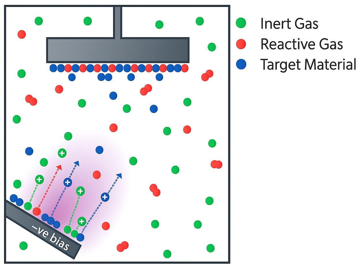
Through sputtering, many different films can be generated from simple metals to complex compounds using elemental or compound targets. Often, when making a compound film, the resultant film stoichiometry (ratio of elements) deposited can differ from the target used due to process limitations. During the sputtering process, the target’s surface is broken up into its constituent elements and vaporised into a largely atomistic flux. Elements in compound films, such as oxygen from oxides and nitrogen from nitride compounds, may be pumped away from the chamber, leaving the film with a lower proportion of oxygen/nitrogen than originally intended.
A key way to combat this issue is through reactive sputtering – this process involves introducing a reactive gas that readily reacts with the deposited film’s surface directly into the vacuum chamber to control the stoichiometry and ensure a fully reacted film.
Reactive sputtering can also provide overall cost efficiencies associated with depositing a film. Generally, RF sputtering supplies have higher capital costs and slower deposition rates than their DC counterparts, but with the added benefit of being able to deposit non-conducting (dielectric) samples. However, reactive DC sputtering can offer a go-around for depositing dielectric films by using a metallic target and introducing a reactive gas to form the compound at the substrate, rather than relying solely on the recombination of the constituent target elements at the correct composition.
Reactive Sputtering FAQs
What is reactive sputtering in PVD?
Reactive sputtering is a variation of Physical Vapour Deposition (PVD) where a reactive gas (such as oxygen or nitrogen) is introduced into the vacuum chamber during the sputtering process. This gas reacts chemically with the sputtered metal atoms to form a compound thin film—typically an oxide, nitride, or carbide—on the substrate.
How does reactive sputtering in PVD work?
- Sputtering Target: A pure metal (e.g., titanium, aluminium, or silicon) is bombarded with high-energy ions (usually from an argon plasma).
- Reactive Gas: A gas like O₂, N₂, or CH₄ is added to the chamber.
- Reaction: The metal atoms ejected from the target react with the reactive gas on the substrate surface.
- Deposition: The resulting compound (e.g., TiO₂, AlN, Si₃N₄) is deposited as a thin film.
What are the applications of reactive sputtering in PVD?
- Optical coatings (anti-reflective layers, interference filters)
- Hard coatings (TiN or diamond-like carbon (DLC) for cutting tools)
- Semiconductor devices (HfOₓ or SiNₓ for passivation or insulation)
- Decorative coatings (colored TiN, ZrN for watches or hardware)
What Are The Advantages of Using reacteive sputtering in PVD?
- Enables deposition of compound films from metallic targets
- Offers fine control over film composition by adjusting gas flow
- Suitable for dense, high-quality coatings
What are the challenges of using reactive sputtering?
- Target poisoning: Excess reactive gas can form a compound layer on the target, reducing sputter efficiency.
- Requires precise process control (gas flow, pressure, plasma power)
What is the difference between reactive sputtering and standard sputtering?
|
Aspect |
Standard Sputtering |
Reactive Sputtering |
|---|---|---|
|
Uses only inert gas |
✅ |
❌ |
|
Forms pure metal films |
✅ |
❌ |
|
Forms compound films |
❌ |
✅ |
|
Needs precise gas control |
❌ |
✅ |

하기