R&D Sources for Thin Film / CIGS / CZTS / CdTe
PEZ Production Effusion Cell
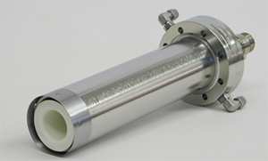
- Flange size 4.5’’ (DN63CF)
- Cell with integrated water cooling on 4.5’’/6’’
- Indirect evaporation for Cu with insert
- Beam shaping, increased material efficiency
- BN liner on request
- Large opening / reduced temperature
- Se resistant shielding
- Se resistant heater
- Protected power feedthrough
Application
The PEZ is especially suited for II-VI semiconductors, CIGS and for Kesteride solar cell material growth.
It allows evaporation of a large number of elements and compounds, including materials such as Se, Ga, Cu, In, NaF, Sn or Zn. The PEZ provides a robust cell design and the consequent optimization of many details leading to a improvement of stability and reproducibility, as well as excellent reliability and easy servicing.
Capacity for the PEZ 63-160-60: 160 ccm crucible for a 30° tilted cell geometry:
|
density |
minimum |
maximum |
|
|
copper |
8,954 g/cm3 |
98 g |
877 g |
|
indium |
7,31 g/cm3 |
95 g |
819 g |
|
gallium |
5,904 g/cm3 |
77 g |
661 g |
The PEZ 63-160 effusion cell is suitable for fast ramping procedures to comparably high deposition rates. With a precise dynamic ramping, the rate profiles of inline deposition systems can be reproduced. Process development and transfer from MBE-like co-evaporation systems to inline production systems become much easier.
A more detailed description you will find in the attached paper (28th EU-PVSEC, 3BV.5.17).
VCS Valved Sulfur Cracking Source
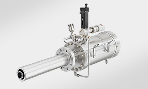
- Provides cracked or uncracked sulfur flux
- Flux modulation and on/off control by motorized valve
- Source capacities from 300 up to 6000 cm³
- Water-cooled assembly
- Excellent flux uniformity due to beam shaping nozzle
- Avoids loss of sulfur during system bakeout
Application
The VCS Valved Sulfur Cracking Source has been designed for the controlled evaporation of sulfur. It can used for II-VI semiconductor thin film research and solar cell manufacturing. Other possible applications are, for example, post-growth sulfurization processes.
MBE-Komponenten provides support in the design of customer-specific research or production systems in order to achieve a customized source geometry, optimized for specified layer uniformity and most efficient deposition material consumption.
Co-deposition processes can be simulated on request. The simulations are based on geometric and Monte Carlo method calculations. Typical results include the lateral layer thickness distribution and material composition for multiple material co-deposition processes on semiconductor wafers as well as on large area substrates.
VSCS Valved Selenium Cracker Source
- Provides cracked or uncracked selenium flux
- Flux modulation and on/off control by motorized valve
- Source capacities from 300 up to 6000 cm³
- Water-cooled assembly
- Excellent flux uniformity due to beam shaping nozzle
- Avoids loss of selenium during system bakeout
Application
The VSCS Valved Selenium Cracking Source has been designed for the controlled evaporation of selenium. It can used for II-VI semiconductor thin film research and solar cell manufacturing. Other possible applications are, for example, post-growth selenization processes with or without carrier gas.
MBE-Komponenten provides support in the design of customer-specific research or production systems in order to achieve a customized source geometry, optimized for specified layer uniformity and most efficient deposition material consumption.
Co-deposition processes can be simulated on request. The simulations are based on geometric and Monte Carlo method calculations. Typical results include the lateral layer thickness distribution and material composition for multiple material co-deposition processes on semiconductor wafers as well as on large area substrates.
