Different Shapes of Sputtering Targets
(주)연진에스텍은 Planar (flat) Target과 Rotary (cylindrical) Target, Circular Target 및 Ring Target 등 대부분의 증착 공정에 부합하는 다양한 형태의 스퍼터링 타겟을 제공하며, 타겟 크기의 커스터마이즈가 가능합니다.
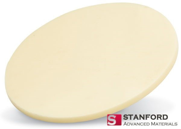
Gallium Nitride Sputtering Targets, GaN
Gallium Nitride Sputtering Targets
Description
Gallium Nitride Sputtering Targets consist of a solid piece or disk made primarily of gallium nitride (GaN), which is a compound semiconductor material. GaN is known for its wide bandgap, high thermal conductivity, and good electrical properties, making it suitable for applications in various electronic devices, such as LEDs, power electronics, and wireless communication systems.
Gallium is a chemical element originated from France (with the Latin name Gallia). It was first mentioned in 1875 and observed by P. E. L. de Boisbaudran. The isolation was later accomplished and announced by P. E. L. de Boisbaudran. “Ga” is the canonical chemical symbol of gallium. Its atomic number in the periodic table of elements is 31 with location at Period 4 and Group 13, belonging to the p-block. The relative atomic mass of gallium is 69.723(1) Dalton, the number in the brackets indicating the uncertainty.
Gallium Nitride Sputtering Targets Specifications
|
Compound Formula |
GaN |
|
Molecular Weight |
83.73 |
|
Appearance |
Yellow Target |
|
Melting Point |
>1600℃ |
|
Density |
6.15 g/cm3 |
|
Available Sizes |
Dia.: 1.0″, 2.0″, 3.0″, 4.0″, 5.0″, 6.0″
Thick: 0.125″, 0.250″ |
Gallium Nitride Sputtering Targets Handling Notes
- Indium bonding is recommended for Gallium Nitride Sputtering Target, due to some of its characteristics not amenable to sputtering like brittleness, low thermal conductivity, etc.
- This material has a low thermal conductivity, and is susceptible to thermal shock.
Gallium Nitride Sputtering Targets Application
Gallium Nitride Sputtering Target is known for its wide bandgap, high thermal conductivity, and good electrical properties, making it suitable for applications in various electronic devices, such as LEDs, power electronics, and wireless communication systems.
Gallium Nitride Sputtering Targets Packaging
Our Gallium Nitride Sputtering Targets are carefully handled during storage and transportation to preserve the quality of our products in their original condition.

- High Purity & Performance 일관된 증착 품질과 오염을 줄이도록 가공합니다.
- Material Variety 다양한 응용 분야의 요구 사항에 맞게 순수 금속, 합금, 세라믹 및 화합물로 제공됩니다.
- Custom Manufacturing 특정 시스템의 필요요구 사항에 맞게 크기와 형태, 조성을 맞춤화했습니다.
- Precision Design 반복 가능하고 균일한 박막 결과를 위해 엄격한 공차로 제조되었습니다.
- Flexible Supply Chain 최고의 제조업체와 강력한 파트너십을 통해 일관된 품질과 on-time 납품을 보장합니다.