Different Shapes of Sputtering Targets
(주)연진에스텍은 Planar (flat) Target과 Rotary (cylindrical) Target, Circular Target 및 Ring Target 등 대부분의 증착 공정에 부합하는 다양한 형태의 스퍼터링 타겟을 제공하며, 타겟 크기의 커스터마이즈가 가능합니다.
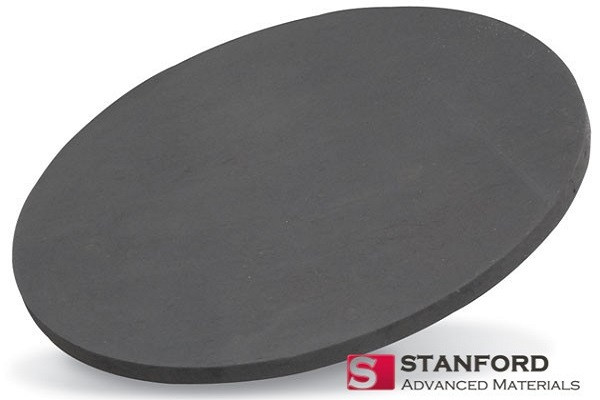
Gallium Antimonide Sputtering Target, GaSb
Gallium Antimonide Sputtering Target
Description
Gallium Antimonide Sputtering Target is a specialized material used in the sputtering process for thin film deposition. In sputtering, high-energy ions are directed at a target material, causing atoms to be ejected from the target surface. These ejected atoms then deposit onto a substrate, forming a thin film with specific properties.
Gallium Antimonide (GaSb) emerges as a versatile semiconductor material, showcasing adjustable conductivity across diverse temperature gradients, thereby proving its suitability for the intricate fabrication of electronic devices. The extraordinary optical properties of Gallium Antimonide contribute to its significance, featuring a bandgap of approximately 0.72 electron volts (eV). This characteristic renders Gallium Antimonide well-matched for the development of sophisticated infrared optics devices and detectors, where precision and sensitivity are paramount. Beyond its electronic and optical prowess, Gallium Antimonide maintains a profile of stable thermal properties across varying temperature ranges. This unique attribute positions Gallium Antimonide as an optimal choice for applications in high-temperature environments, ensuring reliability and performance consistency.
Gallium Antimonide Sputtering Target Specifications
|
Compound Formula |
GaSb |
|
Molecular Weight |
191.48 |
|
Appearance |
Gray Target |
|
Melting Point |
– |
|
Density |
5.62 g/cm3 |
|
Available Sizes |
Dia.: 1.0″, 2.0″, 3.0″, 4.0″, 5.0″, 6.0″
Thick: 0.125″, 0.250″ |
Gallium Antimonide Sputtering Target Handling Notes
- Indium bonding is recommended for the Gallium Antimonide Sputtering Target, due to some of its characteristics not amenable to sputtering like brittleness, low thermal conductivity, etc.
- This material has a low thermal conductivity and is susceptible to thermal shock.
Gallium Antimonide Sputtering Target Application
- Infrared Optics: Gallium Antimonide is widely used in the preparation of infrared optics devices, such as infrared sensors, detectors, and infrared lasers, due to its unique optical properties, especially in the infrared band.
- Electronics: As a semiconductor material, Gallium Antimonide has a wide range of applications in electronics, including field effect transistors (FETs), photodiodes (LEDs), and photodetectors.
- High-Temperature Applications: Gallium Antimonide exhibits excellent and stable thermal properties, making it ideal for high-temperature environments and applications in aerospace, energy, and other high-temperature processes.
- Semiconductor Technology: Because of its semiconductor properties, Gallium Antimonide plays a key role in semiconductor technology, supporting the development of integrated circuits and other semiconductor devices.
Gallium Antimonide Sputtering Target Packaging
Our Gallium Antimonide Sputtering Target is carefully handled during storage and transportation to preserve the quality of our products in their original condition.

- High Purity & Performance 일관된 증착 품질과 오염을 줄이도록 가공합니다.
- Material Variety 다양한 응용 분야의 요구 사항에 맞게 순수 금속, 합금, 세라믹 및 화합물로 제공됩니다.
- Custom Manufacturing 특정 시스템의 필요요구 사항에 맞게 크기와 형태, 조성을 맞춤화했습니다.
- Precision Design 반복 가능하고 균일한 박막 결과를 위해 엄격한 공차로 제조되었습니다.
- Flexible Supply Chain 최고의 제조업체와 강력한 파트너십을 통해 일관된 품질과 on-time 납품을 보장합니다.