Different Shapes of Sputtering Targets
(주)연진에스텍은 Planar (flat) Target과 Rotary (cylindrical) Target, Circular Target 및 Ring Target 등 대부분의 증착 공정에 부합하는 다양한 형태의 스퍼터링 타겟을 제공하며, 타겟 크기의 커스터마이즈가 가능합니다.
Tin Arsenide Sputtering Target, SnAs
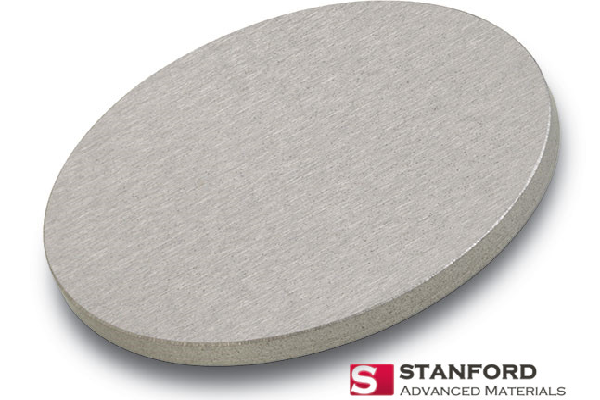
Tin Arsenide Sputtering Target
Description
Tin Arsenide Sputtering Targets, meticulously crafted by Stanford Advanced Materials (SAM), are derived from high-purity Tin Arsenide (SnAs) through precise processing, ensuring fine quality. These targets exhibit exceptional properties, making them suitable for deployment in chemical vapor deposition (CVD) and physical vapor deposition (PVD) processes. The resulting thin films demonstrate excellent performance.
Tin Arsenide (SnAs) stands out as a semiconductor material, finding applications in the realm of electronics and semiconductor devices. With a direct energy gap, Tin Arsenide requires relatively small amounts of energy for electron and hole transitions, rendering it advantageous for select applications in optoelectronics.
Tin Arsenide Sputtering Target Specifications
|
Compound Formula |
SnAs |
|
Molecular Weight |
193.61 |
|
Appearance |
Silver Grey Target |
|
Melting Point |
579 °C |
|
Density |
– |
|
Available Sizes |
Dia.: 1.0″, 2.0″, 3.0″, 4.0″, 5.0″, 6.0″
Thick: 0.125″, 0.250″ |
Tin Arsenide Sputtering Target Handling Notes
- Indium bonding is recommended for Tin Arsenide Sputtering Targets, due to some of its characteristics not amenable to sputtering like brittleness, low thermal conductivity, etc.
- This material has a low thermal conductivity and is susceptible to thermal shock.
Tin Arsenide Sputtering Target Application
Tin Arsenide Sputtering Targets find versatile applications in sputter deposition processes, particularly in the fabrication of semiconductor devices like thin film transistors (TFTs) and various integrated circuit components. Leveraging the semiconductor nature of Tin Arsenide (SnAs), these targets play a crucial role in crafting devices tailored for optoelectronic applications, including the production of photodetectors and lasers. The adaptability of Tin Arsenide Sputtering Targets underscores their significance in the realm of semiconductor technology and optoelectronics.
Tin Arsenide Sputtering Target Packaging
Our Tin Arsenide Sputtering Target is carefully handled during storage and transportation to preserve the quality of our products in their original condition.

- High Purity & Performance 일관된 증착 품질과 오염을 줄이도록 가공합니다.
- Material Variety 다양한 응용 분야의 요구 사항에 맞게 순수 금속, 합금, 세라믹 및 화합물로 제공됩니다.
- Custom Manufacturing 특정 시스템의 필요요구 사항에 맞게 크기와 형태, 조성을 맞춤화했습니다.
- Precision Design 반복 가능하고 균일한 박막 결과를 위해 엄격한 공차로 제조되었습니다.
- Flexible Supply Chain 최고의 제조업체와 강력한 파트너십을 통해 일관된 품질과 on-time 납품을 보장합니다.