Different Shapes of Sputtering Targets
(주)연진에스텍은 Planar (flat) Target과 Rotary (cylindrical) Target, Circular Target 및 Ring Target 등 대부분의 증착 공정에 부합하는 다양한 형태의 스퍼터링 타겟을 제공하며, 타겟 크기의 커스터마이즈가 가능합니다.
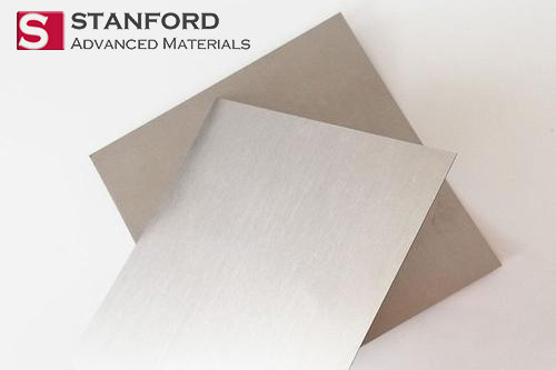
Beryllium Planar Target Be Description
Beryllium Planar Targets are meticulously crafted, high-purity materials showcasing the distinct physical and chemical properties of elemental beryllium. Typically achieving ultra-high purity levels of ≥99.95% (4N5 grade), these targets have trace impurities such as iron, aluminum, and silicon strictly maintained below 50 ppm through advanced purification techniques like zone refining or vacuum distillation. The material’s exceptional thermal conductivity (200 W/(m·K) at room temperature) ensures efficient heat dissipation during high-power sputtering processes, reducing thermal stress and enhancing deposition stability.
Upon exposure to air, a stable, self-passivating beryllium oxide (BeO) layer (~5-10 nm thick) forms spontaneously on the surface, improving corrosion resistance under moderate environmental conditions. However, prolonged exposure to moisture or acidic environments may degrade this protective layer, necessitating storage in inert environments. Microstructurally, the targets are optimized via hot isostatic pressing (HIP) or powder metallurgy to achieve fine grain sizes (<10 µm) and minimal porosity (<0.1%), while surface roughness is refined to Ra < 0.5 µm through diamond turning or chemical-mechanical polishing (CMP).
Safety protocols, including compliance with OSHA 1910.1024 and ISO 17025, govern handling and packaging to mitigate risks from beryllium’s inherent toxicity. Pre-cleaned targets are sealed in inert environments to prevent particulate release. The material’s low coefficient of thermal expansion (11.6 µm/(m·K) at 25°C) ensures compatibility with common substrates like silicon or glass by minimizing thermal mismatch stresses. Rigorous quality validation via XRD, SEM-EDS, and GDMS analysis guarantees consistency, making these targets ideal for applications demanding precision, thermal stability, and ultra-clean deposition performance.
Beryllium Planar Target Be Specification
Properties
- Melting Point: 1277 °C
- Density: 1.848 g/cm³
- Chemical Composition: Be
- Purity Levels: 99%, 99.9%
- Form: Planar
Chemical Composition (%)
|
Element |
Content |
|---|---|
|
Be |
Balance |
|
F |
0.001 |
|
Al |
0.013 |
|
Si |
0.021 |
|
Ti |
0.023 |
|
Cr |
0.029 |
|
Fe |
0.15 |
|
C |
0.05 |
|
O |
0.65 |
The above product information is based on theoretical data. For specific requirements and detailed inquiries, please contact us.
- Size: Customized
Beryllium Planar Target Be Applications
Nuclear Energy & Fusion Technology
Beryllium’s low atomic number (Z=4) and high thermal conductivity (200 W/(m·K)) make it ideal for neutron reflectors and moderators in nuclear reactors. In fusion experimental reactors like ITER, beryllium targets are used to deposit coatings on first-wall armor to withstand extreme plasma radiation (up to 150 million °C). Its oxidation resistance also supports protective layers for nuclear fuel rod cladding.
X-ray & Synchrotron Optics
Beryllium’s near-transparency to low-energy X-rays and neutrons (absorption cross-section ~0.001 barns) enables its use in medical CT detectors, synchrotron beamline windows, and X-ray lithography systems. High-purity (≥99.95%) Be films ensure minimal signal loss and high-resolution imaging.
Aerospace & Space Exploration
With its unmatched specific stiffness (elastic modulus: 287 GPa; density: 1.85 g/cm³), beryllium is critical for satellite structures, space telescope mirrors (e.g., James Webb Space Telescope’s Be mirrors), and rocket nozzle coatings. Its low thermal expansion coefficient (11.6 µm/(m·K)) minimizes deformation in extreme temperatures (-240°C to 300°C), ensuring optical precision.
Semiconductors & Advanced Electronics
Beryllium planar targets facilitate PVD deposition of thermally conductive, low-stress thin films for heat spreaders in high-power electronics. Recent research explores beryllium-based compounds (e.g., BeS) for p-type transparent semiconductors, potentially advancing flexible electronics and optoelectronic devices.
Defense & High-Precision Sensors
Beryllium’s lightweight strength and thermal stability are vital for missile guidance systems, infrared optics, and inertial navigation gyroscopes. Its non-magnetic properties and EMI resistance also enhance performance in hypersensitive sensors for military and aerospace systems.
Specialty Alloys & Industrial Tools
Beryllium-copper alloys (2% Be) are used in non-sparking drilling tools and explosion-proof equipment. Planar targets deposit wear-resistant Be coatings on industrial components, extending service life in corrosive or high-friction environments.
Beryllium Planar Target Be Packaging
Our products are packaged in customized cartons of various sizes based on the material dimensions. Small items are securely packed in PP boxes, while larger items are placed in custom wooden crates. We ensure strict adherence to packaging customization and the use of appropriate cushioning materials to provide optimal protection during transportation.
- Packaging Options: Carton, Wooden Box, or Customized.
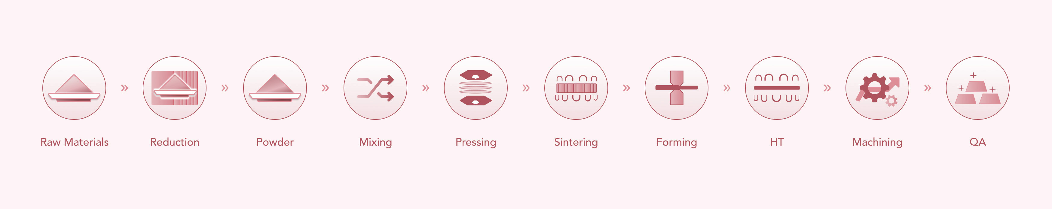
Manufacturing Process
Brief Manufacturing Process Flow
Testing Method
- Chemical Composition Analysis: Verified using techniques such as Glow Discharge Mass Spectrometry (GDMS) or X-ray Fluorescence (XRF) to ensure compliance with purity requirements.
- Mechanical Properties Testing: Includes tensile strength, yield strength, and elongation tests to assess material performance.
- Dimensional Inspection: Measures thickness, width, and length to ensure adherence to specified tolerances.
- Surface Quality Inspection: Checks for defects such as scratches, cracks, or inclusions through visual and ultrasonic examination.
- Hardness Testing: Determines material hardness to confirm uniformity and mechanical reliability.
Beryllium Planar Target Be FAQs
Q1: Why are beryllium targets significantly more expensive than aluminum or copper?
A1:
- Material Scarcity: Global beryllium production is approximately 300 tons per year, with costly purification processes like vacuum distillation and electrolysis.
- Processing Challenges: Beryllium’s brittleness requires specialized methods such as Hot Isostatic Pressing (HIP) or powder metallurgy, which reduce yield.
- Cost-Saving Alternatives: Beryllium-copper alloy targets (0.5-2% Be) offer a 60-80% cost reduction for non-critical applications.
Q2: How should targets or beryllium waste be disposed of?
A2:
- Recycling Service: We offer certified beryllium scrap recycling (priced by weight), compliant with EPA hazardous waste regulations.
- Local Disposal: Clients may use licensed hazardous waste handlers (proof of certification required).
Q3: How is the purity of your beryllium planar targets ensured? Do they meet industry standards?
A3:
- Purity Specifications: Our targets achieve ≥99% purity (2N grade), with critical impurities (e.g., Fe, Al, Si) controlled below 50 ppm, verified via Glow Discharge Mass Spectrometry (GDMS) and X-ray Fluorescence (XRF).
- Certifications: Compliant with ISO 17025 quality standards, supported by third-party test reports (e.g., SGS, UL).
Performance Comparison Table with Competitive Products
Beryllium Target vs. Competing Materials: Performance Comparison
|
Parameter |
Beryllium (Be) |
Aluminum (Al) |
Copper (Cu) |
Titanium (Ti) |
|---|---|---|---|---|
|
Density (g/cm³) |
1.85 |
2.70 |
8.96 |
4.51 |
|
Thermal Conductivity (W/m·K) |
200 |
237 |
401 |
21.9 |
|
Melting Point (°C) |
1287 |
660 |
1085 |
1668 |
|
Sputtering Rate |
Moderate (requires optimized power/gas conditions) |
High (efficient under Ar gas) |
Very high (high sputtering yield) |
Low (requires high power input) |
|
Film Properties |
High hardness, low stress, high thermal stability |
Low resistivity, ductility |
High conductivity, ductility |
High corrosion resistance, biocompatibility |
|
Grain Size Uniformity |
Requires strict process control (nanoscale uniformity) |
Easily controlled (micrometer scale) |
Easily controlled (micrometer scale) |
Requires high-energy sputtering |
|
Toxicity/Safety |
Highly toxic (strict handling required) |
Low toxicity |
Low toxicity |
Low toxicity |
|
Cost (per unit mass) |
Extremely high (rare material + complex processing) |
Low |
Moderate |
Moderate |
|
Key Applications |
Nuclear systems, X-ray windows, aerospace coatings |
Semiconductor interconnects, mirrors |
ICs, conductive layers |
Biomedical coatings, corrosion-resistant layers |
Related Information
Beryllium Element Overview
Beryllium is a lightweight metallic element (atomic number 4, symbol Be) discovered and named in 1798 by the French chemist Vauclain from beryl. As the second lightest metal in the periodic table (with a density of 1.85 g/cm³, after lithium), beryllium exhibits remarkable properties that are not commensurate with its weight. It has a modulus of elasticity of 287 GPa, making it six times tougher than steel, and an extremely high thermal conductivity (200 W/m-K, after silver, copper, and gold). This unique combination of “low density, high stiffness, and high thermal conductivity” makes it a “star material” in extreme industrial scenarios, but its toxicity, high cost, and processing difficulty significantly limit its range of applications.
Core Properties and Scientific Value
Penetration Advantage of Low Atomic Number
Beryllium’s nucleus contains only four protons (Z=4) and has a very low absorption rate for X-rays and neutrons. This property makes it a core material for synchrotron radiation devices, X-ray windows, and an ideal neutron reflecting layer in nuclear reactors. For example, if the X-ray detector window of a medical CT device were made of aluminum or glass, the imaging resolution would be significantly degraded. In contrast, a beryllium window can achieve near-lossless ray penetration with an extremely thin thickness (<1 mm).
Stability in Extreme Environments
Beryllium has a melting point of 1,287°C and maintains a protective layer of beryllium oxide (BeO) at elevated temperatures, providing corrosion resistance that far exceeds that of lighter metals such as aluminum and magnesium. This characteristic has led to its use in high-temperature resistant coatings for rocket nozzles and casing materials for nuclear fuel rods. The U.S. Mars rover Curiosity uses beryllium alloys for its nuclear batteries (RTGs) to withstand the extreme temperatures and radiation on Mars.
An Irreplaceable Role in Aerospace
In satellite and space telescope design, beryllium’s high specific stiffness (stiffness/density) resolves the tension between lightweight and structural strength. For example, the James Webb Space Telescope’s 18 primary mirrors are made of beryllium—a material that has virtually zero deformation in deep space environments at -240°C. Conventional glass or ceramics can distort the image due to thermal expansion and contraction, whereas beryllium maintains optical precision. Similarly, the inertial navigation gyroscopes of intercontinental missiles rely on beryllium components to ensure dimensional stability at high speeds.
Applications and Challenges
Beryllium’s industrial applications are highly concentrated in high-end “must-have” areas:
- Nuclear and Defense: Neutron reducers, nuclear bomb initiators utilizing beryllium’s photo-neutronic reaction properties.
- Precision Optics: High-energy laser mirrors, infrared thermal imager mirror bases.
- Specialty Alloys: Beryllium-copper alloys containing 2% beryllium combine high strength with non-sparking properties for oil and gas drilling tools. These alloys are also used in explosion-proof equipment.

- High Purity & Performance 일관된 증착 품질과 오염을 줄이도록 가공합니다.
- Material Variety 다양한 응용 분야의 요구 사항에 맞게 순수 금속, 합금, 세라믹 및 화합물로 제공됩니다.
- Custom Manufacturing 특정 시스템의 필요요구 사항에 맞게 크기와 형태, 조성을 맞춤화했습니다.
- Precision Design 반복 가능하고 균일한 박막 결과를 위해 엄격한 공차로 제조되었습니다.
- Flexible Supply Chain 최고의 제조업체와 강력한 파트너십을 통해 일관된 품질과 on-time 납품을 보장합니다.