Different Shapes of Sputtering Targets
(주)연진에스텍은 Planar (flat) Target과 Rotary (cylindrical) Target, Circular Target 및 Ring Target 등 대부분의 증착 공정에 부합하는 다양한 형태의 스퍼터링 타겟을 제공하며, 타겟 크기의 커스터마이즈가 가능합니다.
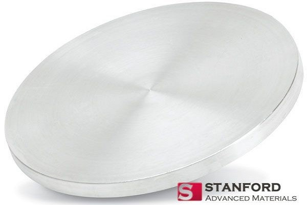
Gallium-Palladium Sputtering Target, GaPd2
Gallium-Palladium Sputtering Target Description
Gallium-Palladium Sputtering Targets exhibit distinctive properties suitable for a diverse range of applications. These targets undergo precision preparation, ensuring high purity and uniformity, establishing a dependable foundation for thin film deposition. The compound’s inherent characteristics position it as a crucial component in electronic, optical, and magnetic materials. Gallium-Palladium Sputtering Targets not only hold promise in semiconductor technology but also showcase unique value in the exploration and fabrication of magnetic materials. Their adaptability renders them highly sought-after for advanced technology and high-tech applications.
By being employed in thin-film preparation, Gallium-Palladium Sputtering Targets play a pivotal role in realizing high-performance electronic devices, optical films, and magnetic applications. In both scientific research and industry, Gallium-Palladium Sputtering Targets underscore their significance in materials science and technological innovation.
Gallium-Palladium Sputtering Target Specifications
|
Compound Formula |
GaPd2 |
|
Molecular Weight |
282.6 |
|
Appearance |
Silver Metallic Target |
|
Melting Point |
– |
|
Density |
– |
|
Available Sizes |
Dia.: 1.0″, 2.0″, 3.0″, 4.0″, 5.0″, 6.0″
Thick: 0.125″, 0.250″ |
Gallium-Palladium Sputtering Target Handling Notes
- Indium bonding is recommended for the Gallium-Palladium Sputtering Target, due to some of its characteristics not amenable to sputtering like brittleness, low thermal conductivity, etc.
- This material has a low thermal conductivity and is susceptible to thermal shock.
Gallium-Palladium Sputtering Target Application
In the realm of electronic, optical, and magnetic materials, GaPd2 stands out as a crucial component due to its inherent characteristics. Beyond its potential in semiconductor technology, Gallium-Palladium Sputtering Targets reveal distinctive value in the exploration and fabrication of magnetic materials, adding to their versatility for advanced technology and high-tech applications.
Gallium-Palladium Sputtering Targets, with their adaptability, become highly sought-after elements for a variety of applications. By playing a pivotal role in thin-film preparation, Gallium-Palladium Sputtering Targets contribute significantly to the realization of high-performance electronic devices, optical films, and magnetic applications. This multifaceted utility underscores the targets’ significance in both scientific research and industry, emphasizing their integral role in materials science and technological innovation.
Gallium-Palladium Sputtering Target Packaging
Our Gallium-Palladium Sputtering Target is carefully handled during storage and transportation to preserve the quality of our products in their original condition.

- High Purity & Performance 일관된 증착 품질과 오염을 줄이도록 가공합니다.
- Material Variety 다양한 응용 분야의 요구 사항에 맞게 순수 금속, 합금, 세라믹 및 화합물로 제공됩니다.
- Custom Manufacturing 특정 시스템의 필요요구 사항에 맞게 크기와 형태, 조성을 맞춤화했습니다.
- Precision Design 반복 가능하고 균일한 박막 결과를 위해 엄격한 공차로 제조되었습니다.
- Flexible Supply Chain 최고의 제조업체와 강력한 파트너십을 통해 일관된 품질과 on-time 납품을 보장합니다.